Switching Mainboard
AssemblyOverview
The switching mainboard is the printed-circuit assembly that does the actual packet work. It hosts the data-plane switching ASIC, the control-plane processor, the memory and lookup resources, and the copper PHYs that drive the front-panel ports.
Construction
A 12-layer Bare PCB provides the controlled-impedance routing that high-speed serial lanes demand. The switching fabric is delivered by a Compute SoC Module sitting at the board's center, surrounded by Ethernet PHY transceivers, six octal devices feeding the 48 access ports. The Control-Plane CPU runs the operating system and routing stack, backed by DDR4 DRAM DRAM and a NAND Flash device holding the boot loader and firmware. Line-rate access-control and route lookups run through dedicated TCAM memory. A Clock Generator supplies the low-jitter reference the serial links need, and extruded Heatsink blocks pull heat off the ASIC and CPU into the forced-air stream.
Switching Mainboard parts and their functions
10 top-level parts · 816 parts in total · full bill of materials below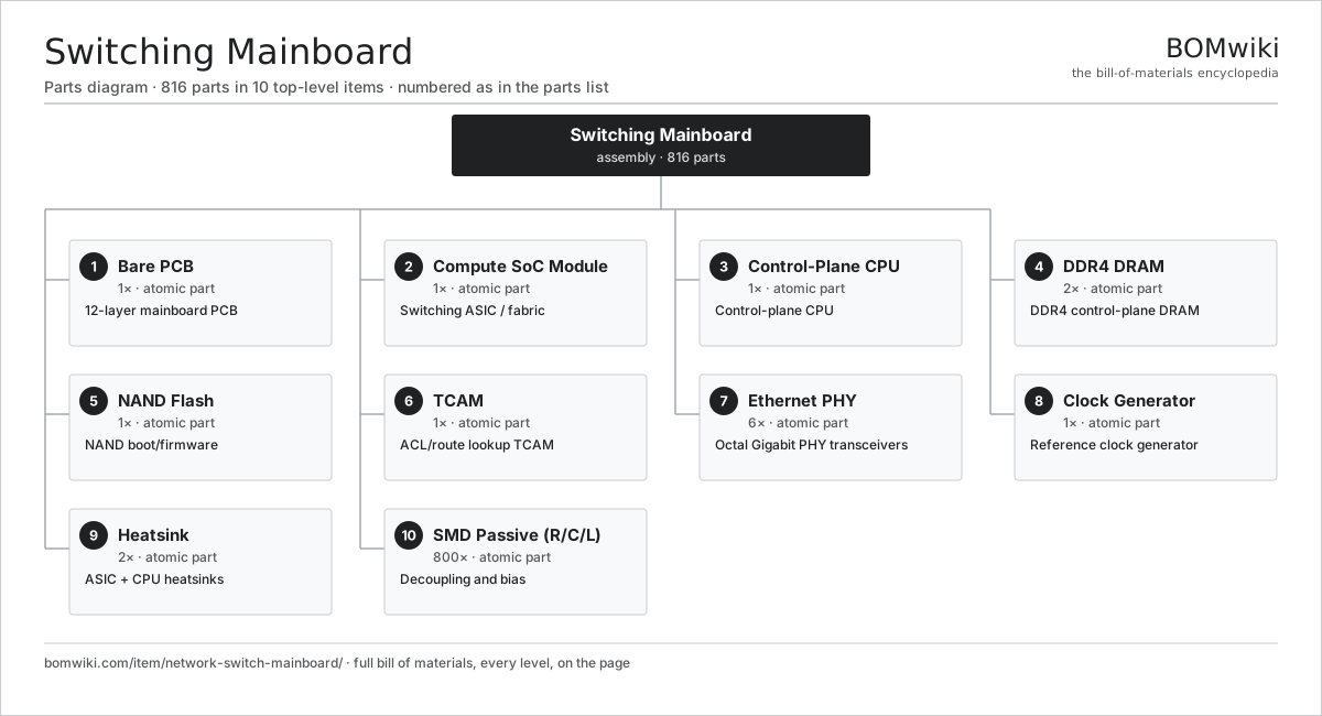
| # | Part | Qty | What it does |
|---|---|---|---|
| 1 | Bare PCB | 1× | 12-layer mainboard PCB |
| 2 | Compute SoC Module | 1× | Switching ASIC / fabric |
| 3 | Control-Plane CPU | 1× | Control-plane CPU |
| 4 | DDR4 DRAM | 2× | DDR4 control-plane DRAM |
| 5 | NAND Flash | 1× | NAND boot/firmware |
| 6 | TCAM | 1× | ACL/route lookup TCAM |
| 7 | Ethernet PHY | 6× | Octal Gigabit PHY transceivers |
| 8 | Clock Generator | 1× | Reference clock generator |
| 9 | Heatsink | 2× | ASIC + CPU heatsinks |
| 10 | SMD Passive (R/C/L) | 800× | Decoupling and bias |
3D model
No 3D model yet. Have a CAD file of this? Add a 3D model. STL renders right on this page; STEP, FreeCAD, and OpenSCAD sources are welcome too (openly licensed, like all 3D models on BOMwiki).
Build & assembly graph
expand / collapse · shared sub-assemblies converge · links to related products · est. labourTap an assembly to expand/collapse · tap a part to open it · use “Open page” for any node · drag to pan, scroll to zoom.
Bill of materials for Switching Mainboard
10 top-level lines · 10 rows shown · 816 parts total · indented to 3 levels| # | Item / sub-assembly | Part no. | Qty/assy | Ext. qty | Parts | Type |
|---|---|---|---|---|---|---|
| 1 | Bare PCB | pcb-bare | 1× | 1 | · | part |
| 2 | Compute SoC Module | soc-module | 1× | 1 | · | part |
| 3 | Control-Plane CPU | network-switch-cpu | 1× | 1 | · | part |
| 4 | DDR4 DRAM | network-switch-ram | 2× | 2 | · | part |
| 5 | NAND Flash | network-switch-flash | 1× | 1 | · | part |
| 6 | TCAM | network-switch-tcam | 1× | 1 | · | part |
| 7 | Ethernet PHY | network-switch-phy | 6× | 6 | · | part |
| 8 | Clock Generator | network-switch-clock-gen | 1× | 1 | · | part |
| 9 | Heatsink | network-switch-heatsink | 2× | 2 | · | part |
| 10 | SMD Passive (R/C/L) | smd-passives | 800× | 800 | · | part |
Something wrong in this list? Report a problem with this BOM.
Where the switching mainboard is used
1 product across 1 domain contain it, directly or inside a sub-assemblyUsed in 1 assembly
Sourcing: possible vendors
Browse the supplier directory → Prices, MOQ, and lead times are algorithmic estimates, not quotes, and not claims about these companies. Company mappings are curated by keyword; est. price band $1–$200. How estimates work| Vendor | HQ | Specialty | MOQ | Lead time |
|---|---|---|---|---|
|
🇨🇳JLCPCB
jlcpcb.com ↗
|
Shenzhen, CN | PCB fabrication | 100 pcs | 2–4 wks |
|
🇨🇳PCBWay
pcbway.com ↗
|
Shenzhen, CN | PCB fab & assembly | 100 pcs | 2–4 wks |
| scc.com.cn ↗ | Shenzhen, CN | PCB manufacturer | 100 pcs | 2–4 wks |
| shogini.com ↗ | Mumbai, IN | PCB manufacturer | 100 pcs | 2–4 wks |
| venture.com.sg ↗ | Singapore | Electronics contract mfg | 100 pcs | 2–4 wks |
162-word article